The 2026 GPU Field Guide: H200, B200, B300, GB200, GB300, Vera Rubin, MI3xx and Helios, From the Chip to the Rack
6,465 words · 32 min read
Disclaimer: This post reflects my personal views and does not represent the views of my employer or my community.
Lead image generated with Grok. Figures 1 to 9 are my own drawings from public NVIDIA, AMD and Oracle documentation. Every number has a reference at the bottom; where a vendor has not published one, I say so in the text.
Related readings from this blog:
- Three Weeks in Batam: Bringing NVIDIA GB200 to Life on the Data Plane - where I met my first NVL72 rack
- GPU Burn-In at Scale - what to run on this hardware before you trust it
- The Complete NCCL Reference Guide - the software side of the NVLink and RDMA fabrics described here
- RDMA, RoCEv2 and InfiniBand Explained to a Ten-Year-Old - the scale-out network, from the beginning
- From First Principles to Zettascale - how OCI designed the RDMA network these GPUs sit on
- OCI at NVIDIA GTC 2025 and Oracle AI World 2025 - where most of these SKUs were announced for OCI
- Build the Data Centers - why the watts and water section matters more than the FLOPS
Executive Summary
I have seen it many times at OCI when we work on new SKUs for our AI frontier customers (xAI, OpenAI, Meta). Understanding and translating a vendor datasheet (AMD or NVIDIA) is very different from the reality of a hyperscaler data center. Turning what the datasheet promises into engineering numbers that make sense has been my career at my current employer. For the last seven years I have worked on each generation of GPU, mostly through experimentation, trial and error, and testing.
This blog is a blueprint for how all the SKUs fit together, and a collection of my experience on the ground. It is the document I would have loved to have when I flew to Indonesia to launch OCI’s first GB200 at scale, the first launch of a rack-level GPU at scale in the world. I try to cover all the big SKUs: NVIDIA H100, H200, B200 and B300, the two rack-level NVL72 systems (GB200 and GB300), and the new Vera Rubin NVL72, which OCI intends to be first to launch at scale again. I cover the AMD SKUs as well: MI300X, MI325X, MI350X, MI355X, and the MI455X, which is a rack-level SKU inside Helios. I go from the chip design to the rack and I focus on the hardware: memory, links, watts, air or water, which network, the coverage and the limits, and the commands I run before I sign off that a machine is healthy. This is a follow-up to my burn-in guide and the NCCL guide, both linked above. Together the three give you the full picture of a mission that is fundamental to everyone working in a hyperscaler on GPUs: the best infrastructure for frontier models, so they can produce the best AI models for the world.
As in all my documents, I finish each section as I would explain it to a ten-year-old. It matches my mental model of first principles, and the line often attributed to Einstein: if you can’t explain it to your nana, you don’t understand it.
Table of Contents
- How to Read a SKU Name
- The Chip: What Is Inside One Package
- The Box: Eight GPUs and How They Talk
- The Rack: When the Rack Became the Computer
- The SKU Tables
- Watts and Water
- Networks: Scale-Up, Scale-Out, and the Reference Architecture
- Which SKU for Which Job
- What Breaks, With Numbers
- Five Minutes of Commands: Prove What the Truck Delivered
- The Ten Commandments
- References
How to Read a SKU Name
GB200 NVL72. The first time I heard those letters in the OCI Seattle office, I sweated as I wondered what the heck I had signed up for. Whoever named it at NVIDIA had a funny love of car plates from the state of NVL. Later, after reading the NVIDIA documents and going through their excellent training program for preferred partners, I realised it is not random. It is a code, and once you know the science behind it, it lets you work out the components of the rack from the name alone. I will show you how to decipher this Da Vinci code.
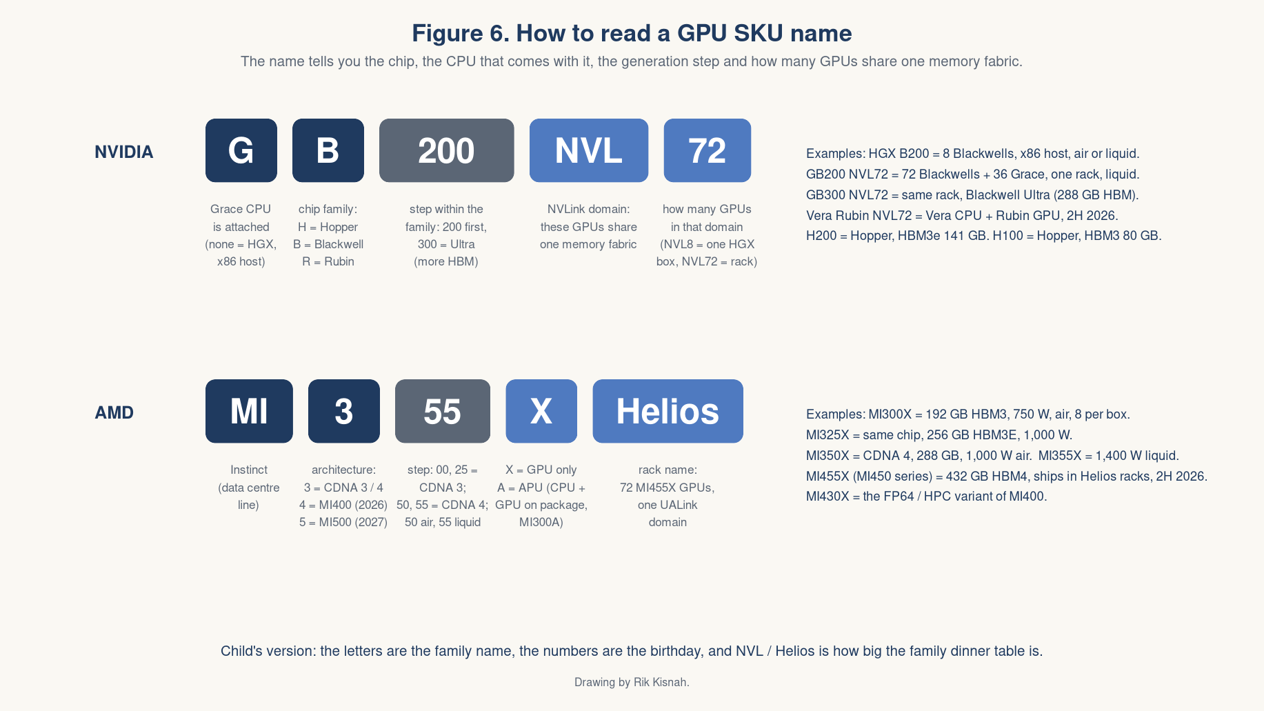
Let us look at NVIDIA naming first. The first letter is the chip family: H is Hopper, B is Blackwell, R is Rubin. A G in front means a Grace Arm CPU is soldered on the same board as the GPU. On an HGX baseboard we do not see a G, because it fits in an ordinary x86 server, the type you have seen before in regular compute. The number is the step inside that family, and 300 (as in B300 or GB300) means “Ultra”: the same silicon with more HBM (High Bandwidth Memory), and the tensor cores rebalanced for low-precision inference. NVL with a number is how many GPUs share one NVLink memory fabric. NVL8 is one box, and NVL72 is one rack. That number matters to architects because it tells them whether a repair is limited to one server or involves a one-tonne cabinet, which changes the whole supply chain plan.
AMD is one of my favourite vendors, because the company is open source; everything they do is available to the world, and I love that about them. MI is the Instinct data center product line. As with NVIDIA, the first digit is the architecture generation (3 covers CDNA 3 and CDNA 4, and 4 is the MI400 series, which we are now working to release to the world). The next two digits are the step, and within the step, the 0 model is air cooled and the 5 model is liquid cooled: MI350X uses air, MI355X uses water. X means GPU only. A means an APU with CPU cores on the package, which is what runs El Capitan.
What is CDNA? Compute DNA, AMD’s data-center-only GPU architecture (compute, no graphics). “DNA” is just AMD’s branding for an architecture family, with no deeper meaning. AMD’s separate gaming architecture is RDNA, and the two share little despite the similar name.
Explain it to a ten-year-old. The letters are the family name, the numbers are the birthday, and NVL72 or Helios tells you how many cousins share one dinner table.
The Chip: What Is Inside One Package
The first time I looked at a Blackwell die (it was in the lab, on an RMA machine; trust me, once you open a GB200 you void the warranty on a million-dollar SKU, so do not try this at home), I was a bit surprised, because it is not a single chip. Most modern AI SKUs have more than one silicon die glued together, and the software and drivers make it look like one device. Always read the datasheet to see how this wiring works, so you are not surprised when you get to low-level debugging. I will walk through some of the nuances here.
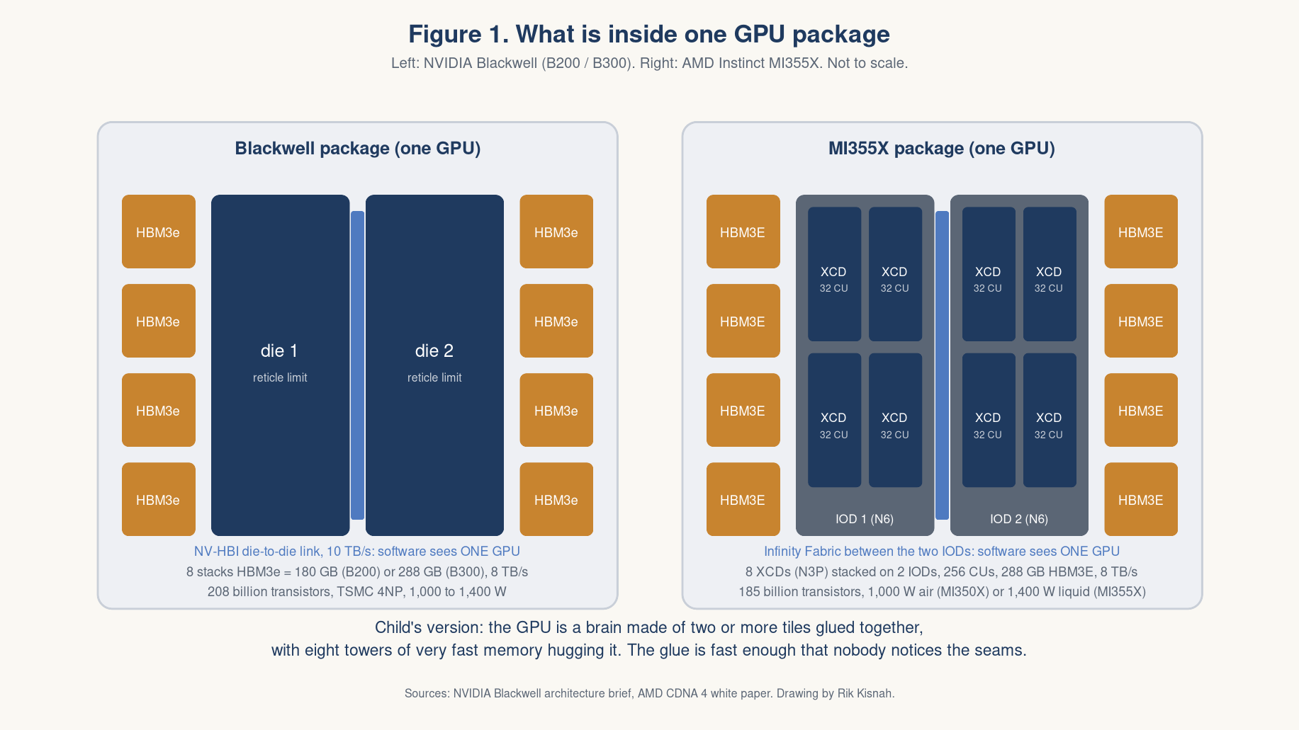
Blackwell (B200, B300, and the GPU half of GB200 and GB300) is two chips working as a single chip. Each chip is printed in a single shot, which is what “reticle-limited” means: a tongue twister, but an engineering feat, because it is the largest single chip that can be made today. NVIDIA prints two of those maximum-size dies and links them with a fast connection called NV-HBI, at 10 TB/s, so they act as one bigger GPU instead of two separate ones [1].
More needs to be said about the packaging. It holds 208 billion transistors, thanks to TSMC’s 4NP manufacturing process, and fast memory (HBM3e) seated beside the dies. B200 comes with 180 GB of that fast memory. The 300 series, B300 and GB300, comes with 288 GB. Both move data at 8 terabytes per second; at that speed you could copy the whole text of English Wikipedia about 300 times every second [1][2][3]. The Rubin series, due in the second half of 2026, keeps the same two-chip design but has 336 billion transistors and a new memory type, HBM4, with 288 GB running at 22 terabytes per second, almost three times faster than Blackwell [4].
AMD pursued this multi-chip design as well and, contrary to popular belief, started earlier than NVIDIA. MI300X was built from twelve separate pieces of silicon (a Frankenstein design, and it works): eight compute chips, called XCDs (accelerator complex dies), seated on top of four connector chips, the IODs (I/O dies), with 153 billion transistors in total [5]. MI350X and MI355X have a simpler and cleaner design: eight compute chips on just two connector chips, which streamlines manufacturing, with 185 billion transistors and eight taller memory stacks giving 288 GB at 8 terabytes per second [6]. MI455X, the chip in the Helios rack, takes the engineering further: twelve memory stacks for 432 GB at 23.3 terabytes per second [7]. That is a lot of memory packed together, and keeping it at a safe temperature is a real challenge, because silicon starts to fail above a certain temperature.
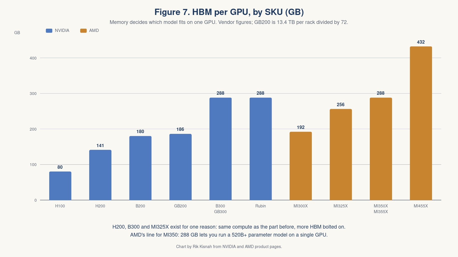
Memory is the product in AI data centers. Compute doubles every generation (Huang’s law, a funny stab at Moore’s law). HBM determines which models fit on one GPU and how many GPUs a job needs, and that number matters to AI training and inference engineers more than any other. The H100 has 80 GB, the H200 has 141 GB, and the B300 and Rubin have 288 GB. MI455X has 432 GB. AMD’s own line for the MI350 series is that 288 GB lets you run a 520B+ parameter model on a single GPU [6]. Memory is why AI training labs rent machines: to run a model inside a supercomputer with fast memory, and the more HBM there is, the more you can pack in. You could argue memory matters more than FLOPS. I do.
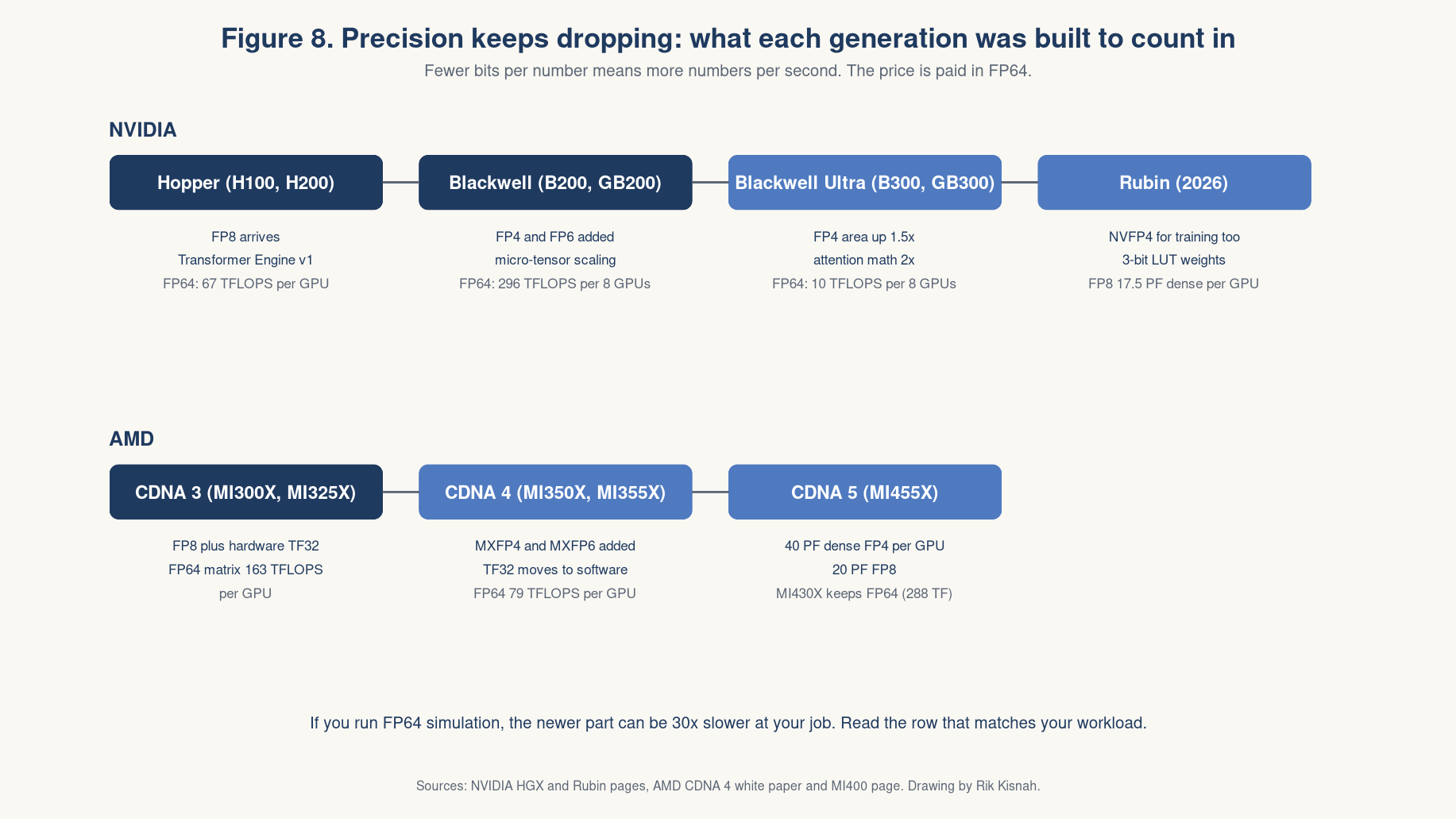
Precision is always dropping. For chips, that means they are designed to do maths with fewer bits per number, trading accuracy for speed. Hopper introduced FP8 (8-bit numbers). Blackwell added FP4 and FP6 (4-bit and 6-bit). HGX B300 promises 108 PFLOPS of dense FP4, with only 10 TFLOPS of FP64 (the older, more precise 64-bit format), compared with 296 TFLOPS of FP64 on HGX B200 [2]. If you read the details you might wonder why a more expensive chip is slower than the older generation. TL;DR: a business and pragmatic reason. Chip space is limited, so NVIDIA shrank the high-precision units to make room for the AI maths (FP4 and FP6), which is more than sufficient for training and inference. New chips are faster, but slower at old-school precise maths. AMD made the same call. CDNA 4 added its own flavour of low-precision formats (MXFP4 and MXFP6) and pushed out the older TF32, so the hardware no longer handles it natively [6]. Same business decision as NVIDIA.
Explain it to a ten-year-old. The GPU is a brain made of tiles glued together, hugged by eight towers of very fast memory. The glue is so fast nobody notices the seams. Newer brains count with shorter numbers, so they can count more per second.
The Box: Eight GPUs and How They Talk
Inside a server, eight GPUs talk to each other faster than any network could carry the data. NVIDIA and AMD solved this in two different ways.
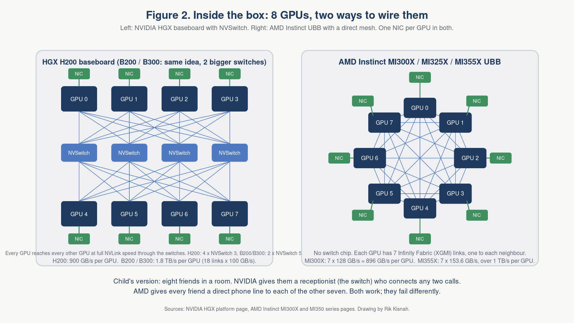
NVIDIA HGX places eight GPUs on a baseboard with NVSwitch chips in the middle, so every GPU reaches every other GPU at full NVLink speed: 900 GB/s per GPU on H100 and H200, and 1.8 TB/s per GPU on B200 and B300, which have 18 links at 100 GB/s each [1][2][8]. HGX H200 carries four third-generation NVSwitch chips. HGX B200 and B300 carry two fifth-generation NVLink switches with 14.4 TB/s of total NVLink bandwidth [2]. The downside is that when a switch dies, all eight GPUs lose bandwidth, and in my experience the training job usually notices before the telemetry picks it up.
AMD UBB puts eight OAM modules on a baseboard too, but with no switch chip. Instead, each GPU connects directly to all seven others in a full mesh over Infinity Fabric links. On MI300X and MI325X each link runs at 128 GB/s, for 896 GB/s per GPU [5]. On MI350X and MI355X the newer links run at 153.6 GB/s, which AMD rounds up to “over 1 TB/s” per GPU [6]. An eighth link is reserved as PCIe Gen5 x16 up to the host. A dead link here only hurts one pair of GPUs; RCCL routes around it, so the collective slows down instead of stopping outright.
Both designs give each GPU its own back-end NIC, and both need that NIC sitting under the same PCIe root complex as its GPU, so GPUDirect RDMA never has to cross the CPU. This is the “rail” I keep bringing up in the NCCL guide. Run nvidia-smi topo -m or rocm-smi --showtopo to check whether the box you actually received was built that way. Always check. Integrators make mistakes with riser cables.
Explain it to a ten-year-old. Eight friends in a room. NVIDIA gives them a receptionist who can connect any two calls. AMD gives each friend a direct line to the other seven. When the receptionist is off sick, nobody talks. When one AMD line is cut, two friends have to shout across the room.
The Rack: When the Rack Became the Computer
With GB200 NVL72, the unit you buy, test and repair stopped being a server and became a rack. I wrote about that experience in Batam, where we wrote the runbook for the world. Helios now does the same thing for AMD, so it is worth understanding what a rack-scale SKU actually is.
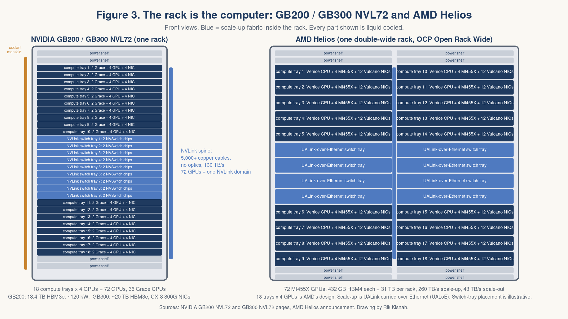
GB200 NVL72 and GB300 NVL72. One rack holds 18 compute trays and 9 NVLink switch trays. Each compute tray carries two superchips, meaning two Grace CPUs, four Blackwell GPUs, and their NICs [9]. Each switch tray carries two NVSwitch chips with “144 NVLink ports at 100 GB” [9]. The trays meet at a copper-cable spine in the back of the rack, with no optics anywhere, giving 72 GPUs in one NVLink domain with 130 TB/s of aggregate bandwidth [10][11]. A GPU on tray 3 reads HBM on tray 15 through IMEX, NVIDIA’s Internode Memory Exchange service, which “supports GPU memory export and import (NVLink P2P) and shared memory operations across OS domains” [12]. GB200 gives the rack 13.4 TB of HBM3e. GB300 gives it 20 TB and ConnectX-8 SuperNICs at 800 Gb/s per GPU [10][11]. Vera Rubin NVL72 keeps the 18 plus 9 layout and doubles the fabric to 260 TB/s with NVLink 6 at 3.6 TB/s per GPU [4][13].
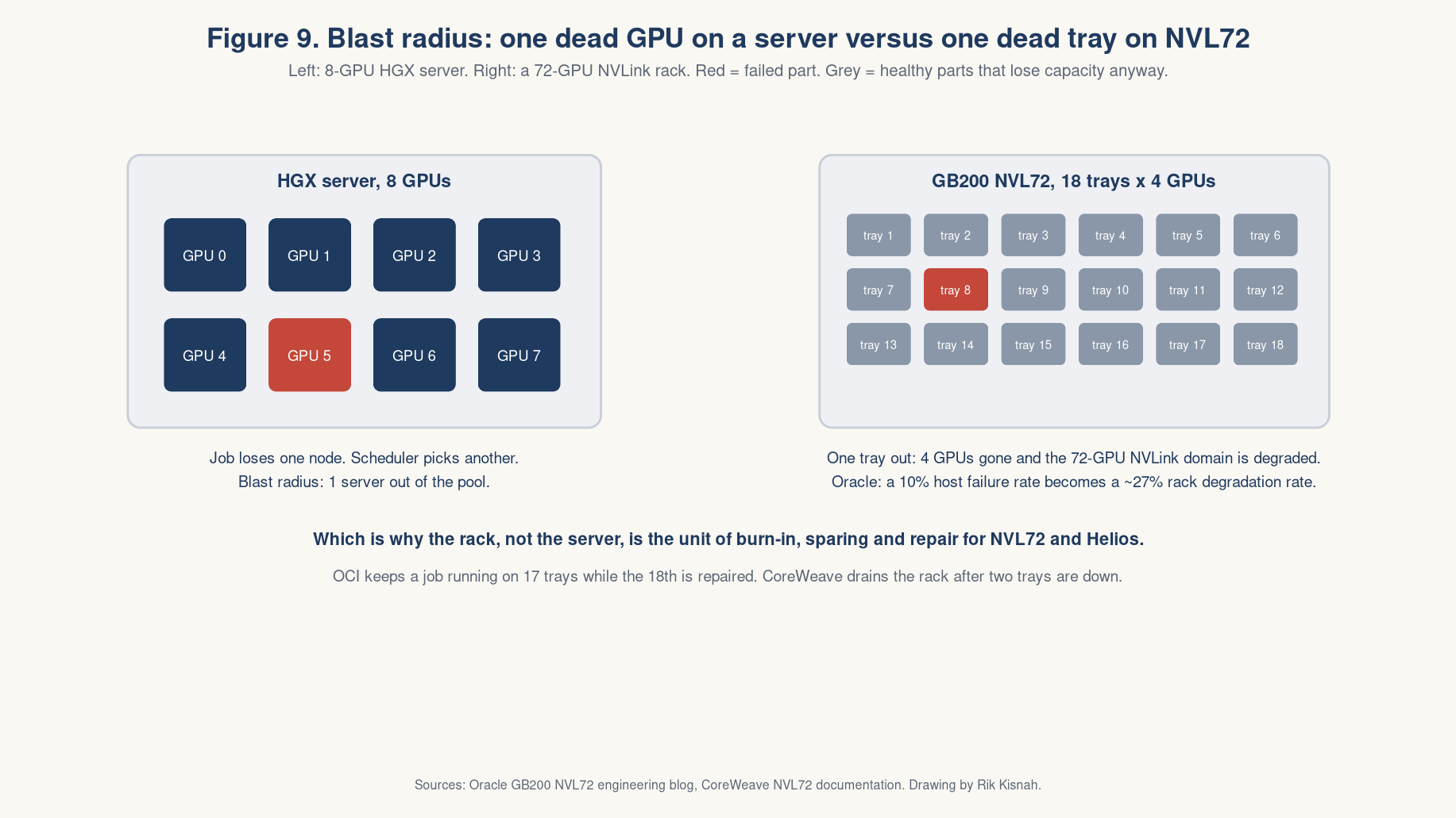
On an 8-GPU server, a dead GPU costs you one node. On NVL72, a dead tray degrades the rack, and OCI’s own GB200 engineering blog puts a number on it: “a 10% host failure rate exacerbates to ~27% rack degradation rate” [14]. I covered this in more depth in the burn-in guide, along with why OCI built APIs to keep a job running on 17 trays while the 18th is out for repair [14]. CoreWeave tells its customers to design for two nodes down per rack, after which the whole rack gets drained [15]. Plan for that on day one, not after the first ticket.
Helios. AMD’s rack holds 72 MI455X GPUs in 18 trays of four, each tray with one EPYC “Venice” CPU and three Pensando Vulcano 800G NICs per GPU [7][16]. Scale-up is UALink tunneled over Ethernet (AMD calls it UALoE) through four copper cartridges and switch trays with “two 512 lane 200G UALoE switch ASICs” each, for 260 TB/s, exactly the Vera Rubin figure and not by accident [16]. It lives in Meta’s double-wide Open Rack Wide with a vertical busbar and a quick-disconnect liquid manifold [16]. AMD says Helios is “now in production” as of July 2026 with volume in the second half, and is careful to add that it is “a reference design, not a product for sale”: the OEMs build it [7][16]. Oracle has committed to 50,000 MI450-series GPUs in Helios racks from calendar Q3 2026 [17], and I do plan to write about it once it has shipped.
Explain it to a ten-year-old. Before, each computer was a box. Now the whole cupboard is the computer, and when one shelf breaks, the cupboard limps.
The SKU Tables
The money tables, from OCI, NVIDIA and AMD public documents. Figures are per GPU unless marked otherwise. Tensor FLOPS use dense numbers where the vendor publishes them. I have split each vendor into two parts, “the silicon” and “the site”, because that is how these conversations actually play out: one with the ML team, a separate one with the facilities team.
NVIDIA, the silicon
| SKU | Unit | HBM per GPU | HBM bandwidth | Scale-up per GPU | FP4 dense / FP8 dense per GPU |
|---|---|---|---|---|---|
| H100 SXM | HGX 8-GPU | 80 GB HBM3 | 3.35 TB/s | NVLink 4, 900 GB/s | none / ~2 PF |
| H200 SXM | HGX 8-GPU | 141 GB HBM3e | 4.8 TB/s | NVLink 4, 900 GB/s | none / ~2 PF |
| B200 | HGX 8-GPU | 180 GB HBM3e | 8 TB/s | NVLink 5, 1.8 TB/s | 9 / 4.5 PF |
| B300 | HGX 8-GPU | 288 GB HBM3e | 8 TB/s | NVLink 5, 1.8 TB/s | 13.5 / 4.5 PF |
| GB200 NVL72 | 72-GPU rack | 186 GB (13.4 TB per rack) | 8 TB/s | NVLink 5, 1.8 TB/s; 130 TB/s per rack | 10 / 5 PF (720 / 360 PF per rack) |
| GB300 NVL72 | 72-GPU rack | 288 GB (20 TB per rack) | 8 TB/s | NVLink 5, 1.8 TB/s; 130 TB/s per rack | 15 / 5 PF (1,080 / 360 PF per rack) |
| Vera Rubin NVL72 | 72-GPU rack | 288 GB HBM4 (20.7 TB per rack) | 22 TB/s | NVLink 6, 3.6 TB/s; 260 TB/s per rack | 50 PF NVFP4 inference; 17.5 PF FP8 dense |
NVIDIA, the site
| SKU | Power | Cooling | Back-end NIC | OCI shape | Status |
|---|---|---|---|---|---|
| H100 SXM | 700 W | air | ConnectX-7 400G | BM.GPU.H100.8 | shipping [18] |
| H200 SXM | 700 W | air | ConnectX-7 400G | BM.GPU.H200.8 | shipping [8] |
| B200 | 1,000 W (OEM figure) | air or liquid | ConnectX-7 400G | BM.GPU.B200.8 | shipping [2][19] |
| B300 | not published | air or liquid | ConnectX-8 800G on the baseboard | BM.GPU.B300.8 | shipping [2][3] |
| GB200 NVL72 | ~120 kW per rack | direct liquid | ConnectX-7 400G; ConnectX-8 2x400G on OCI v3 | BM.GPU.GB200.4 | shipping [10][14][20] |
| GB300 NVL72 | 132 kW per rack nominal (OEM figure) | direct liquid | ConnectX-8 800G | BM.GPU.GB300.4 | shipping [11] |
| Vera Rubin NVL72 | ~200 kW per rack (reported) | direct liquid, 45 °C inlet | 2 x ConnectX-9 800G per GPU | not yet listed | in production, ships 2H 2026 [4][13][21] |
AMD, the silicon
| SKU | Unit | HBM per GPU | HBM bandwidth | Scale-up per GPU | FP4 dense / FP8 dense per GPU |
|---|---|---|---|---|---|
| MI300X | UBB 8-GPU | 192 GB HBM3 | 5.3 TB/s | 7 x 128 GB/s Infinity Fabric | none / 2.6 PF |
| MI325X | UBB 8-GPU | 256 GB HBM3E | 6 TB/s | 7 x 128 GB/s | none / 2.6 PF |
| MI350X | UBB 8-GPU | 288 GB HBM3E | 8 TB/s | 7 x 153.6 GB/s | 9.2 / 4.6 PF |
| MI355X | UBB 8-GPU | 288 GB HBM3E | 8 TB/s | 7 x 153.6 GB/s | 10.1 / 5 PF |
| MI455X / Helios | 72-GPU rack | 432 GB HBM4 (31 TB per rack) | 23.3 TB/s | UALoE 3.6 TB/s; 260 TB/s per rack | 40 / 20 PF (2.9 / 1.4 EF per rack) |
AMD, the site
| SKU | Power | Cooling | Back-end NIC | OCI shape | Status |
|---|---|---|---|---|---|
| MI300X | 750 W | air | 8 x 400G | BM.GPU.MI300X.8 | shipping [5] |
| MI325X | 1,000 W | air | 8 x 400G | none | shipping [22] |
| MI350X | 1,000 W | air | Pollara 400 or 400G | none | shipping [6] |
| MI355X | 1,400 W | direct liquid, 43 °C inlet | Pollara 400 or 400G | BM.GPU.MI355X.8 | shipping [6][23] |
| MI455X / Helios | not published (225 to 245 kW per rack reported) | direct liquid | 3 x Vulcano 800G per GPU | 50,000 GPUs from Q3 2026 | in production July 2026 [7][16][17] |
Three footnotes that will save you an argument. NVIDIA product pages quote sparse FLOPS by default and dense in brackets; AMD quotes dense. NVIDIA’s “50 PFLOPS” for Rubin is an NVFP4 inference figure, and AMD’s comparison chart puts MI455X’s 40 PF dense FP4 against 35 PF for Rubin on the same basis [7], so do not let a vendor compare its dense number to the other side’s sparse one. And neither vendor publishes watts per GPU for the rack SKUs; the rack figures above are OEM or integrator numbers plus OCI’s plain statement that “each GB200 rack can draw over 120 kW at peak” [14].
Watts and Water
The chip is no longer the hard part. The building is. I made that argument at length in Build the Data Centers; here is the version with the numbers per SKU.
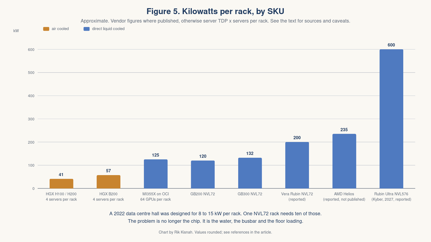
A DGX B200 is “~14.3 kW max” in 10 rack units, and it is still air cooled [19]. Four of those in a rack is close to 60 kW, which already exceeds most enterprise halls. GB200 NVL72 is about 120 kW in one rack, all direct-to-chip liquid, because, as OCI’s GB200 blog puts it, “air cooling is no longer viable at this scale” [14]. GB300 adds energy storage in the power shelves to smooth the synchronous spikes a training job produces, which NVIDIA says cuts peak grid demand by up to 30% [11]. Vera Rubin NVL72 is designed for 45 °C warm-water inlet [13], and the Rubin Ultra rack planned for 2027 is reported at roughly 600 kW. Six hundred. I remember when 20 kW was a “high density” rack.
AMD lands in the same place by a different road. MI350X at 1,000 W stays air cooled, so it drops into an existing 120 to 130 kW rack at 64 GPUs. MI355X at 1,400 W is liquid only, 96 to 128 GPUs in a “properly configured 200 kW” rack [6]. OCI’s MI355X racks hold 64 GPUs at 125 kW [23]. AMD publishes the coolant spec for MI355X, which I wish everyone did: PG-25 glycol, maximum inlet 43 °C, 2.1 litres per minute per GPU module [24]. Helios rack power is NDA only; The Register reports 225 to 245 kW under load.
I first saw direct liquid cooling in OCI’s Utah and Indonesia data centers, and it is impressive engineering with rigorous science behind it. It also changes your job. In the order you will meet each one:
- Leak test and flow check before power. Do not rack a rack until the loop holds pressure and every tray shows nominal flow. Quick-disconnects are the weak point; log every mate and unmate like a cable event.
- Inlet temperature is a spec, not a preference: 45 °C for NVIDIA MGX racks, 43 °C for MI355X. Warmer water means cheaper chillers and less headroom when something goes wrong.
- Thermal faults look like performance faults. A cold plate with a bubble in it does not alarm. It throttles. Watch
clocks_event_reasons.activeandamd-smi metric --throttle, not just temperatures, or you will chase a “slow GPU” for a week. - The busbar is the new single point of failure. NVL72 and Helios feed trays from a vertical DC busbar through power shelves. A shelf fault is a rack fault.
- Floor loading. An NVL72 rack weighs about 1.36 tonnes. Check the slab before the truck arrives, not after.
Explain it to a ten-year-old. Old computers were cooled by blowing on them, like hot soup. These need water pipes, like a car engine. One cupboard uses as much electricity as fifty houses.
Networks: Scale-Up, Scale-Out, and the Reference Architecture
Two networks exist, and confusing them is the most common design mistake I see in architecture reviews. It usually shows up as someone quoting NVLink bandwidth for a job that spans four racks.
Scale-up is the memory fabric: NVLink inside a box or a rack, Infinity Fabric inside a UBB, UALink inside Helios. It is copper, short, and measured in terabytes per second per GPU. Scale-out is the RDMA fabric between boxes or racks: InfiniBand or RoCEv2 Ethernet, optical beyond a few metres, measured in hundreds of gigabits per GPU. OCI’s GB200 blog states the split in one sentence: “The NVLink domain is used as the scale-up network within a rack, and the InfiniBand or RoCE RDMA network is then used as the scale-out network across racks” [14]. If RDMA is new to you, start with my RDMA, RoCEv2 and InfiniBand explainer.
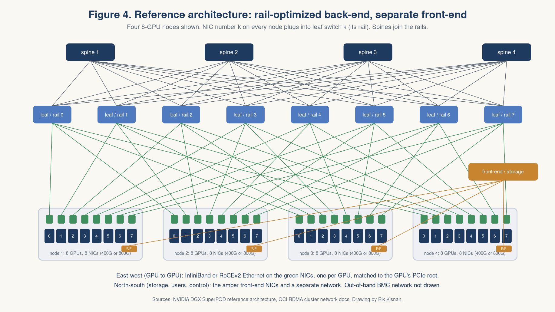
The reference architecture is the same on both vendors, which tells you it is physics and not marketing. One back-end NIC per GPU. NIC number k on every node plugs into leaf switch k, its “rail”, so the GPUs that talk most in a collective are one hop apart, and spines join the rails. NVIDIA’s HGX AI Factory design calls this “2-8-9-400”: two CPUs, eight GPUs, nine NICs, 400 Gb/s [25]. AMD’s MI3XX reference design offers the same rail topology or a fat tree on RoCEv2, up to 8,192 GPUs [26]. A separate front-end network carries storage, users and control, and a third, out-of-band, carries the BMCs. NVIDIA’s DGX SuperPOD documents list exactly those four fabrics [27]. The burn-in guide tests each one differently; this is why.
InfiniBand or RoCEv2. NVIDIA sells both: Quantum-X800 InfiniBand at 800G with 144 ports per switch for dedicated SuperPODs, and Spectrum-X Ethernet for multi-tenant clouds, with adaptive routing and congestion control coordinated between switch and SuperNIC [28][29]. AMD is Ethernet only, and its RoCE guide gives the recipe without hedging: DCQCN, “achieved by enabling two features, Explicit Congestion Notification (ECN) and Priority Flow Control (PFC)”, RoCE traffic on DSCP 26, congestion notification packets on DSCP 48, MTU 9216 [30]. The Ultra Ethernet Consortium 1.0 specification of June 2025 is where both camps’ Ethernet NICs are heading [31].
NICs you will see
| NIC | Speed | Host bus | Where |
|---|---|---|---|
| NVIDIA ConnectX-7 | 400G, InfiniBand or Ethernet | PCIe Gen5 | HGX H100, H200, B200; GB200 NVL72; OCI H100, H200, B200 shapes |
| NVIDIA ConnectX-8 SuperNIC | 800G | PCIe Gen6 | HGX B300 (on the baseboard), GB300 NVL72, OCI GB200 v3 [3][20] |
| NVIDIA ConnectX-9 | 800G, two per GPU | PCIe Gen6 | Vera Rubin NVL72 [13] |
| NVIDIA BlueField-3 / 4 DPU | 400G | PCIe Gen5 / Gen6 | front-end and storage in DGX systems |
| AMD Pensando Pollara 400 | 400G, UEC-ready, RoCEv2 | PCIe Gen5 | MI350 racks; OCI is first to deploy it on the back end [32] |
| AMD Pensando Vulcano 800 | 800G, UEC 1.0, three per GPU | PCIe Gen6 and UALink | Helios [16] |
OCI’s design, since it is the public reference I know best: RoCEv2 on ConnectX NICs, a three-tier Clos with “400 Gbps nonblocking connectivity to each GPU” up to 131,072 GPUs [33]. I covered the first-principles thinking behind it in From First Principles to Zettascale. The Acceleron multiplanar design that Pradeep Vincent, Jag Brar and David Becker presented in October 2025 connects each NIC to four switches on four isolated planes, so a bad plane costs you bandwidth, not the job [34]. Optics and cables have been the bane of my life for two years, and multiplanar is the first design I have seen that treats a flapping optic as normal weather rather than an outage.
Explain it to a ten-year-old. Inside the cupboard the shelves talk through thick copper straws. Between cupboards they talk through thin glass threads. Straws are faster. Threads reach further.
Which SKU for Which Job
Vendor positioning in the vendor’s own words, translated into what an infrastructure team should actually order. I have left the marketing quotes in on purpose, so you can see what the vendor is optimising for.
| Job | Buy | Why, in the vendor’s framing |
|---|---|---|
| Fine-tuning and inference of models up to about 70B on one GPU | H200, MI300X, MI325X | H200 is “the GPU for generative AI and HPC” with 141 GB [8]; MI300X was “the only option capable of running inference for a 70B parameter model on a single accelerator” at launch [5] |
| Dense inference at lowest cost per token, models to 500B on one GPU | B300, MI355X | 288 GB each; AMD claims “up to 40% more tokens-per-dollar” [6]; B300 doubles attention throughput and carries 800G NICs [2] |
| Pretraining at hundreds to thousands of GPUs in air-cooled halls | B200, MI350X | 1,000 W air-cooled drop-ins with FP4 and 8 TB/s HBM [2][6] |
| Trillion-parameter training and real-time MoE inference | GB200 NVL72 | “30x faster real-time trillion-parameter LLM inference”; 72 GPUs share memory so expert parallelism stays on NVLink [10] |
| Reasoning and test-time-scaling inference | GB300 NVL72 | “a single massive GPU built for test-time scaling” [11] |
| Agentic inference and MoE training with the fewest GPUs, 2H 2026 | Vera Rubin NVL72, Helios | NVIDIA: “4x reduction in number of GPUs to train MoE models” [21]; AMD: “up to 30% more tokens per dollar than the leading competitive solution” [7] |
| FP64 simulation and HPC | H100, H200, B200, MI300A, MI430X in 2027 | B300 and GB300 cut FP64 to 10 TFLOPS per 8 GPUs; MI430X targets “288 TFLOPS peak hardware-based FP64” [7] |
| Million-token context prefill | Rubin CPX | “purpose-built for massive-context processing”, 128 GB GDDR7 [35] |
What Breaks, With Numbers
No vendor publishes a per-SKU annual failure rate, and anyone who quotes you one over a beer is guessing. What we do have is the public record, and it is better than people think. The burn-in guide covers the bathtub curve and the test pipeline; this section is about what the curve looks like for each SKU.
The baseline, from Meta’s Llama 3 run. 16,384 H100s for 54 days: 466 interruptions, 419 of them unexpected, about 78% attributed to hardware [36]. The top rows of their table:
| Cause | Count | Share |
|---|---|---|
| Faulty GPU | 148 | 30.1% |
| GPU HBM3 memory | 72 | 17.2% |
| Software bug | 54 | 12.9% |
| Network switch or cable | 35 | 8.4% |
| GPU SRAM | 19 | 4.5% |
| NIC | 7 | 1.7% |
Scale does the rest. Meta’s HPCA 2025 study of 24,000 A100s found an 8-GPU job fails on average every 47.7 days, a 1,024-GPU job every 7.9 hours, and projects 1.8 hours at 16,384 GPUs and 14 minutes at 131,072 [37]. The hardware did not get worse. There was simply more of it in each job. The NCSA Delta study found H100 HBM3 has a per-GPU mean time between uncorrectable memory errors 3.2x worse than A100’s HBM2e, and recommends 5% overprovisioning to hold 99.9% job availability [38]. Imbue’s 4,088-GPU cluster arrived with about 10% of machines failing to boot, then broke at about 3% of machines per week, most of the pain in InfiniBand transceivers [39]. Every one of those numbers matches what I have seen on the floor.
What changes per SKU
| SKU family | What I expect to fail first | Why |
|---|---|---|
| H100 / H200 HGX | HBM (Xid 48, 94, 95), GPUs falling off the bus (Xid 79), optics | Delta and Meta data above; 64 HBM stacks per node |
| B200 / B300 HGX | Same list, plus thermal throttling and power-related resets | 1,000 to 1,400 W per GPU in chassis designed for 700 W airflow |
| GB200 / GB300 NVL72 | NVLink backplane and cartridge links, coolant quick-disconnects, rack blast radius | Oracle’s 10% host to 27% rack figure [14]; SemiAnalysis reports the copper backplane “still is not that reliable” after burn-in (secondary) [40] |
| MI300X / MI325X | HBM temperature and XGMI link errors | SemiAnalysis attributes a higher rate than H100/H200 to “higher temperatures and less mature Samsung HBM” (secondary, no data) [41] |
| MI355X | Liquid loop and 1,400 W power delivery | New cold plates, 43 °C inlet, AMD’s first liquid-only generation [24] |
| MI455X / Helios | Unknown; new UALoE cartridges and 216 NICs per rack | Three 800G NICs per GPU is three times the optics count of an NVL72 |
| Vera Rubin NVL72 | Unknown; first HBM4 and first 200 kW-class rack | New memory, new power density |
Two rules follow, and I repeat them in every review. Measure change, not state: a GPU with 50 corrected ECC errors from the factory is not news; one that gains 50 during a four-hour run is. And rack SKUs need rack-level acceptance: OCI tests “every GPU-to-GPU connection across all 72 Blackwell GPUs” through the NVLink switch before a GB200 rack is handed over [14]. If your vendor did not do that, do it yourself before the first customer job lands on it.
Explain it to a ten-year-old. If one toy in a hundred is broken and you buy a thousand, ten are broken before you open the box. If all thousand have to hold hands to play, the game stops every time one lets go.
Five Minutes of Commands: Prove What the Truck Delivered
Run these on the first node of every delivery, save the output, and diff it after burn-in. The comments say what each SKU should report. I have been burned by every line in here at least once, which is how they earned their place.
# What chip, how much HBM, what power cap
nvidia-smi --query-gpu=name,memory.total,power.limit,vbios_version --format=csv
#  H100 SXM 81559 MiB 700 W | H200 143771 MiB 700 W | B200 ~183 GB 1000 W | B300 / GB300 ~288 GB

# NVLink: count active links and their speed
nvidia-smi nvlink -s
#  Hopper: 18 links x 26.5 GB/s per direction (900 GB/s total)
#  Blackwell: 18 links x 50 GB/s per direction (1.8 TB/s total)

# NVL72 only: is this GPU in the rack fabric, and does IMEX see all 18 trays?
nvidia-smi -q | grep -A4 Fabric          # State: Completed, Status: Success
nvidia-imex-ctl -N                       # every node READY

# Which NIC sits under which GPU (the rail map)
nvidia-smi topo -m
# AMD: chip, HBM, links, host bus
amd-smi static --asic --vram --board      # MI300X 192 GB | MI325X 256 GB | MI355X 288 GB
amd-smi xgmi                              # 7 links per GPU, all up
sudo lspci -d 1002: -vvv | grep -E "LnkSta"   # Speed 32GT/s, Width x16, no FatalErr+
amd-smi metric --power --temperature --throttle   # MI355X can run at 1400 W; throttle must be clear
# The back-end fabric: which NIC, which speed, InfiniBand or RoCE
ibstat | grep -E "CA '|Rate|Link layer|State"
#  ConnectX-7: Rate 400, Link layer Ethernet -> RoCEv2 (OCI); Link layer InfiniBand -> NDR
#  ConnectX-8: Rate 800 (B300, GB300, OCI GB200 v3)
rdma link                                 # every back-end port ACTIVE
ethtool <iface> | grep -E "Speed|Link"    # Pensando Pollara 400000Mb/s, Vulcano 800000Mb/s

# RoCEv2 essentials on a ConnectX port: PFC, trust mode, ECN
mlnx_qos -i eth1
cat /sys/class/net/eth1/ecn/roce_np/enable/*

# Errors that identify a bad part (snapshot before and after every run)
dmesg -T | grep -i "NVRM: Xid"            # 48/94/95 memory, 74 NVLink, 79 fell off the bus
nvidia-smi -q -d ECC,ROW_REMAPPER | grep -E "Uncorrectable|Pending|Failure"
nvidia-smi nvlink -e                      # CRC, replay, recovery counters
amd-smi metric --ecc --ecc-blocks         # UMC block = HBM
amd-smi bad-pages                         # retired HBM pages
mlxlink -d /dev/mst/mt4129_pciconf0 -c -e # NIC port BER and eye
What the numbers should be
| Check | H100 / H200 | B200 | B300 / GB300 | GB200 | MI300X | MI355X |
|---|---|---|---|---|---|---|
| GPUs visible per host | 8 | 8 | 8, or 4 per tray | 4 per tray | 8 | 8 |
| HBM per GPU | 80 / 141 GB | 180 GB | 288 GB | 186 GB | 192 GB | 288 GB |
| NVLink or XGMI links up | 18 | 18 | 18 | 18, fabric State Completed | 7 | 7 |
| PCIe to host | Gen5 x16 | Gen5 x16 | Gen6 x16 | Gen5 x16 | Gen5 x16 | Gen5 x16 |
| Back-end ports and rate | 8 x 400 | 8 x 400 | 8 x 800 | 4 x 400 (v3: 4 x 2 x 400) | 8 x 400 | 8 x 400 |
| Power cap | 700 W | 1,000 W | vendor | vendor | 750 W | 1,400 W |
The Ten Commandments
- The name is a code: family letter, generation number, 300 means more HBM, NVL or Helios means the rack is the computer.
- Buy memory first. HBM capacity decides how many GPUs a job needs; compute headlines decide how fast it finishes.
- FP4 is the new headline and FP64 got cut on B300 and GB300. Read the row that matches your workload, not the one on the slide.
- NVIDIA boxes fail at the switch. AMD boxes fail at a link. Rack SKUs fail at the rack.
- Above 1,000 W per GPU, plan for water: 45 °C inlet for NVIDIA MGX racks, 43 °C PG-25 for MI355X.
- One back-end NIC per GPU, rail-optimized, 400G today and 800G on B300, GB300 and Helios. Front-end and BMC on separate networks.
- InfiniBand or RoCEv2 both work. RoCEv2 needs ECN and PFC on every hop, and UEC 1.0 is where both vendors’ Ethernet NICs are going.
- Expect a few percent of nodes bad on arrival (Imbue saw 10%) and about 3% breaking per week early in life. HBM and optics are the top two causes.
- At 1,024 GPUs a job fails every 8 hours. At 131,072 it is every 14 minutes. Checkpoint accordingly.
- Run the five minutes of commands on delivery and again after burn-in. The delta is the evidence. Everything else is opinion.
References
- NVIDIA Blackwell architecture: https://www.nvidia.com/en-us/data-center/technologies/blackwell-architecture/
- NVIDIA HGX platform (B200 and B300 tables): https://www.nvidia.com/en-us/data-center/hgx/
- NVIDIA developer blog, Inside Blackwell Ultra: https://developer.nvidia.com/blog/inside-nvidia-blackwell-ultra-the-chip-powering-the-ai-factory-era/
- NVIDIA developer blog, Inside the Rubin GPU architecture: https://developer.nvidia.com/blog/inside-nvidia-rubin-gpu-architecture-powering-the-era-of-agentic-ai/
- AMD Instinct MI300X page, datasheet, CDNA 3 white paper and launch release: https://www.amd.com/en/products/accelerators/instinct/mi300/mi300x.html , https://www.amd.com/content/dam/amd/en/documents/instinct-tech-docs/white-papers/amd-cdna-3-white-paper.pdf , https://ir.amd.com/news-events/press-releases/detail/1173/
- AMD Instinct MI350 series, MI355X page and CDNA 4 white paper: https://www.amd.com/en/products/accelerators/instinct/mi350.html , https://www.amd.com/en/products/accelerators/instinct/mi350/mi355x.html , https://www.amd.com/content/dam/amd/en/documents/instinct-tech-docs/white-papers/amd-cdna-4-architecture-whitepaper.pdf
- AMD Instinct MI400 series page and Advancing AI 2026 release: https://www.amd.com/en/products/accelerators/instinct/mi400.html , https://ir.amd.com/news-events/press-releases/detail/1294/
- NVIDIA H200: https://www.nvidia.com/en-us/data-center/h200/
- NVIDIA developer blog, GB200 NVL72 delivers trillion-parameter LLM training and real-time inference: https://developer.nvidia.com/blog/nvidia-gb200-nvl72-delivers-trillion-parameter-llm-training-and-real-time-inference/
- NVIDIA GB200 NVL72: https://www.nvidia.com/en-us/data-center/gb200-nvl72/
- NVIDIA GB300 NVL72 and Blackwell Ultra release: https://www.nvidia.com/en-us/data-center/gb300-nvl72/ , https://nvidianews.nvidia.com/news/nvidia-blackwell-ultra-ai-factory-platform-paves-way-for-age-of-ai-reasoning
- NVIDIA IMEX guide: https://docs.nvidia.com/multi-node-nvlink-systems/imex-guide/overview.html
- NVIDIA DGX Vera Rubin NVL72 (preliminary) and Vera Rubin POD blog: https://www.nvidia.com/en-us/data-center/dgx-vera-rubin-nvl72/ , https://developer.nvidia.com/blog/nvidia-vera-rubin-pod-seven-chips-five-rack-scale-systems-one-ai-supercomputer/
- Oracle, Behind the scenes: NVIDIA GB200 NVL72 on OCI: https://blogs.oracle.com/cloud-infrastructure/behind-the-scenes-nvidia-gb200-nvl72-oci-apis
- CoreWeave NVL72 documentation: https://docs.coreweave.com/docs/platform/instances/nvl72
- AMD Helios page, launch blog (July 2026) and Vulcano NIC blog: https://www.amd.com/en/products/rackscale-solutions/helios.html , https://www.amd.com/en/blogs/2026/amd-launches-helios-the-highest-performing-rackscale-ai-infrastructure-solution.html , https://www.amd.com/en/blogs/2026/amd-pensando-vulcano-800-ai-nic-scale-out-and-across.html
- Oracle and AMD, MI450 supercluster: https://www.oracle.com/news/announcement/ai-world-oracle-and-amd-expand-partnership-to-help-customers-achieve-next-generation-ai-scale-2025-10-14/
- NVIDIA H100: https://www.nvidia.com/en-us/data-center/h100/
- NVIDIA DGX B200 and Lenovo HGX B200 product guide (180 GB, 1,000 W): https://www.nvidia.com/en-us/data-center/dgx-b200/ , https://lenovopress.lenovo.com/lp2226
- Oracle, OCI achieves NVIDIA Exemplar Cloud on GB200 NVL72 (BM.GPU.GB200v3.4): https://blogs.oracle.com/cloud-infrastructure/oci-achieves-nvidia-exemplar-cloud-nvidia-gb200
- NVIDIA Rubin platform releases, CES and GTC 2026: https://nvidianews.nvidia.com/news/rubin-platform-ai-supercomputer , https://nvidianews.nvidia.com/news/nvidia-vera-rubin-platform
- AMD Instinct MI325X: https://www.amd.com/en/products/accelerators/instinct/mi300/mi325x.html
- Oracle, MI355X general availability and June 2025 AMD release (125 kW, 64 GPUs per rack): https://blogs.oracle.com/cloud-infrastructure/announcing-general-availability-of-oci-amd-mi355x , https://www.oracle.com/news/announcement/oracle-and-amd-collaborate-to-help-customers-deliver-breakthrough-performance-for-large-scale-ai-and-agentic-workloads-2025-06-12/
- AMD Instinct MI355X platform brochure (coolant PG-25, 43 °C, 2.1 l/min): https://www.amd.com/content/dam/amd/en/documents/instinct-tech-docs/product-briefs/amd-instinct-miI355x-platform-brochure.pdf
- NVIDIA HGX AI Factory reference architecture: https://docs.nvidia.com/enterprise-reference-architectures/hgx-ai-factory-h100-h200-b200/latest/index.html
- AMD Instinct MI3XX reference design: https://instinct.docs.amd.com/projects/MI3XX-reference/latest/index.html
- NVIDIA DGX SuperPOD reference architectures, GB200 and B200: https://docs.nvidia.com/dgx-superpod/reference-architecture-scalable-infrastructure-gb200/latest/index.html , https://docs.nvidia.com/dgx-superpod/reference-architecture-scalable-infrastructure-b200/latest/index.html
- NVIDIA Quantum-X800: https://networking-docs.nvidia.com/xdrswitcheshw/introduction
- NVIDIA Spectrum-X: https://www.nvidia.com/en-us/networking/spectrumx/
- AMD RoCE network configuration guide: https://instinct.docs.amd.com/projects/cluster-documentation/latest/how-to/roce-network-config.html
- Ultra Ethernet Consortium specification 1.0: https://ultraethernet.org/ultra-ethernet-consortium-uec-launches-specification-1-0-transforming-ethernet-for-ai-and-hpc-at-scale/
- AMD Pensando Pollara 400 product brief: https://www.amd.com/content/dam/amd/en/documents/pensando-technical-docs/product-briefs/pollara-product-brief.pdf
- Oracle, First Principles: Inside zettascale OCI Superclusters: https://blogs.oracle.com/cloud-infrastructure/first-principles-zettascale-oci-superclusters
- Oracle, First Principles: Oracle Acceleron multiplanar networking: https://blogs.oracle.com/cloud-infrastructure/first-principles-acceleron-multiplanar-networking
- NVIDIA Rubin CPX release: https://nvidianews.nvidia.com/news/nvidia-unveils-rubin-cpx-a-new-class-of-gpu-designed-for-massive-context-inference
- Grattafiori et al., The Llama 3 Herd of Models, section 3.3.4 and Table 5: https://arxiv.org/abs/2407.21783
- Kokolis et al., Revisiting Reliability in Large-Scale Machine Learning Research Clusters, HPCA 2025: https://arxiv.org/abs/2410.21680
- Cui et al., Story of Two GPUs: Characterizing the Resilience of Hopper H100 and Ampere A100 GPUs, SC 2025: https://arxiv.org/abs/2503.11901
- Imbue, From bare metal to a 70B model: https://imbue.com/research/70b-infrastructure/
- SemiAnalysis, H100 vs GB200 NVL72 training benchmarks (secondary): https://newsletter.semianalysis.com/p/h100-vs-gb200-nvl72-training-benchmarks
- SemiAnalysis, ClusterMAX rating system (secondary, paywalled): https://newsletter.semianalysis.com/p/the-gpu-cloud-clustermax-rating-system-how-to-rent-gpus
- Oracle compute shapes (all OCI shape names and RDMA bandwidths): https://docs.oracle.com/en-us/iaas/Content/Compute/References/computeshapes.htm
- Rik Kisnah, GPU Burn-In at Scale: https://www.rik-kisnah.ai/posts/gpu-burn-in-at-scale-reference-guide/ and The Complete NCCL Reference Guide: https://www.rik-kisnah.ai/posts/nccl-complete-reference-guide/